basic_example
Welcome to FPGA world!
- In this section we will learn how to use the FPGA board and how to program it. We assume that you have almost zero knowledge about FPGA and we will try to explain everything from scratch. We will use the DE10-LITE FPGA board from Terasic. The are tens of FPGA boards in the market with lots of different features, but we will use this one because it is cheap and it has a lot of nice things that satisfied our goals.
Open Quartus project
- In that section we will make a basic design of pushing a button and lighting a LED.
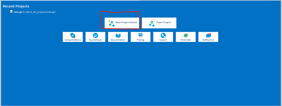
Open quartus and select a new project by clicking on New Project Wizard
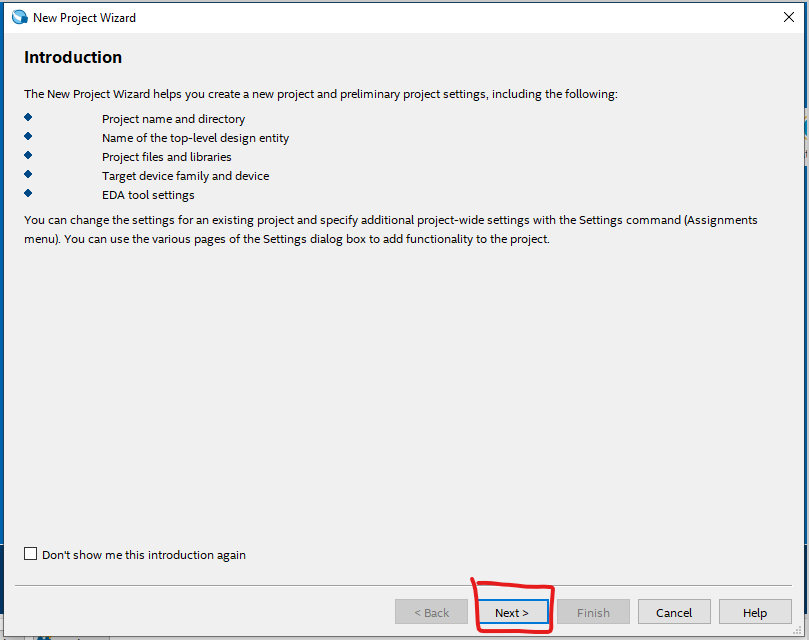
If that window appears, click on Next.
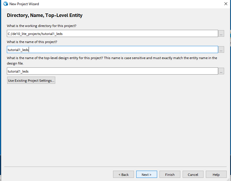
Choose a name for your project and a folder click on Next.
- We recommend you to create a new and empty folder for your project.
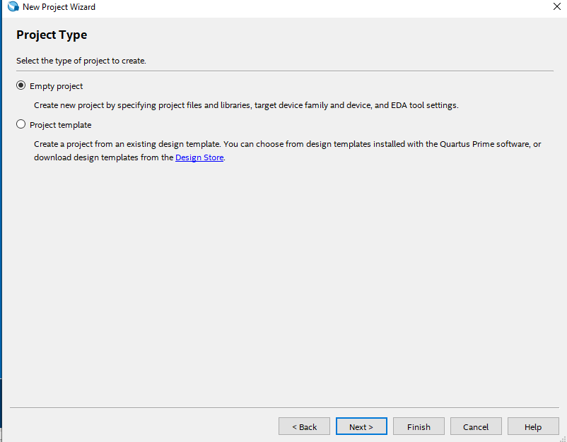
If that window appears, click on Next.
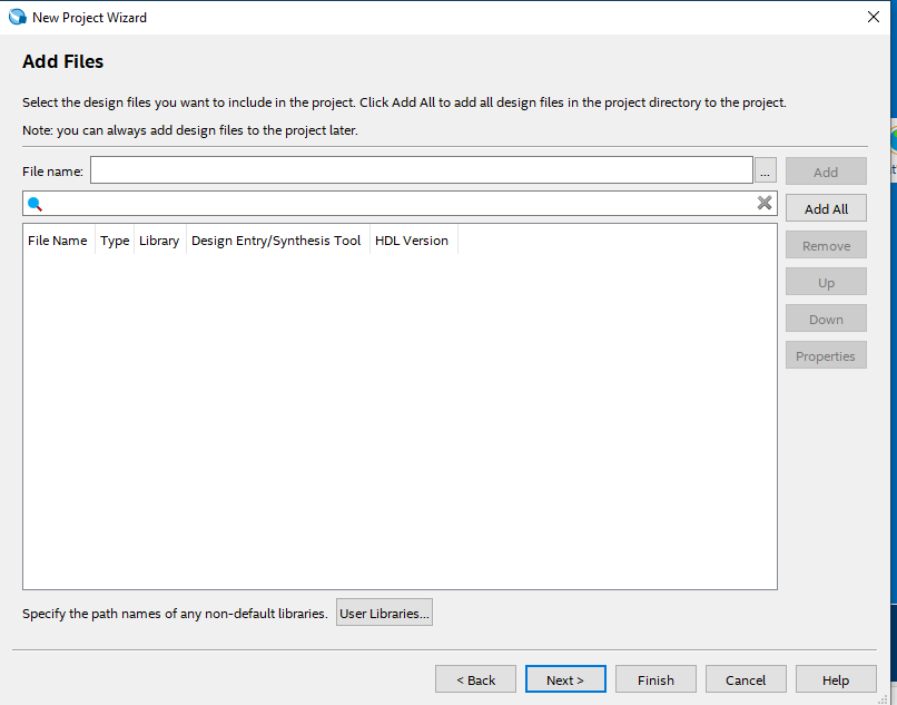
At that point we wont add any files to our project, so click on Next.
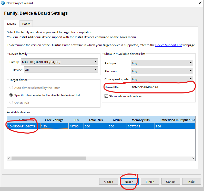
That window is very important. You have to choose the FPGA board that you will use. In our case we will use the DE10-LITE board, Please type 10M50DAF484C7G in the right field and select it. Then click on Next.
- That number represents the FPGA chip that is used in the DE10-LITE board.
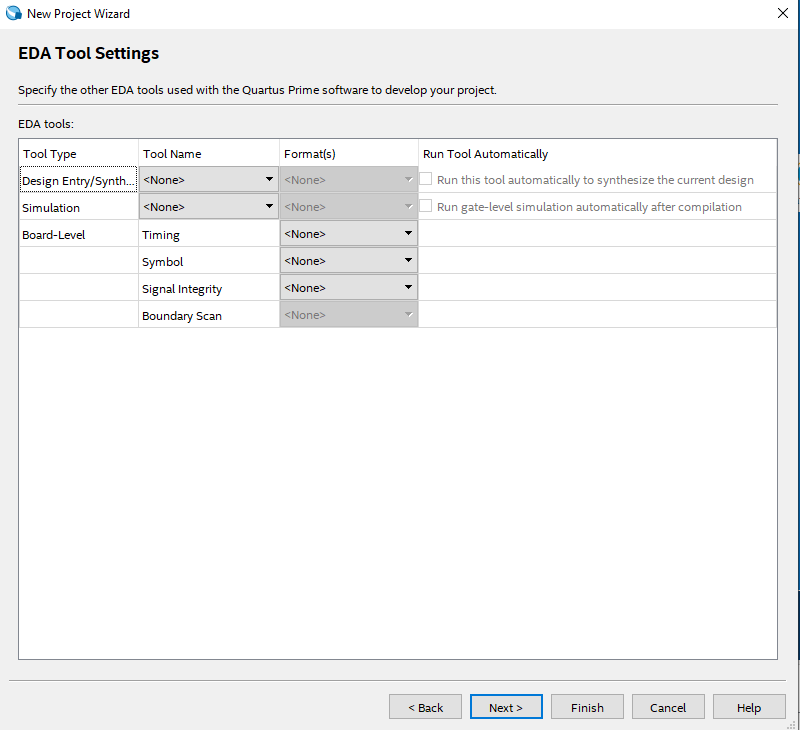
If that window appears, click on Next.
If that summary window, click on Finish.

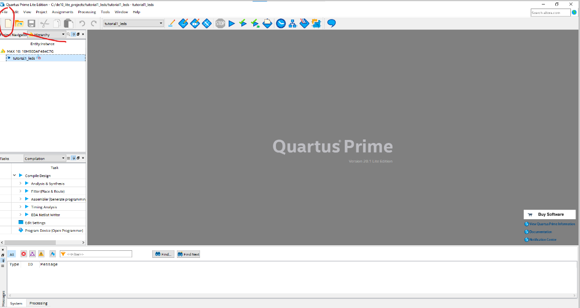
Adding files and compilation
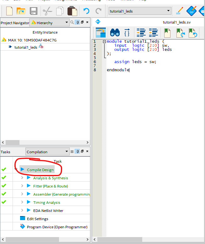
To add file click on the left side icon and than select SystemVerilog HDL file and click on OK.
Add the following code to the file and save it.
- make sure that the top module name has the same name as the file name.
module tutorial1_leds (
    input  logic [2:0] sw,
    output logic [2:0] leds
);

    assign leds = sw;

endmodule
- To compile the file double click on compilation and wait until the compilation is finished. You will see a green check mark if the compilation is successful. Compilation is a process that converts the code that you wrote to hardware on the fpga. It also performs place and route, which means that it decides where the hardware will be placed on the fpga and how the hardware will be connected.
Pin assignment
- In that section we will assign the pins of the fpga to the inputs and outputs of our design. For example we need to connect the leds in our design to the pins of the fpga that are connected to the leds.
- Go to assignment -> pin planner. The following window will appear.

At the button of the window you can see the inputs and the outputs of your design. You can press the
Node Nameto switch the order of the pins.Download de10 lite manual from here and open it. You can also find it on google without open the terasic official site.
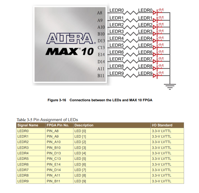
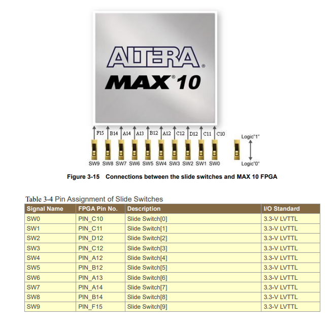
Assign the pins in the following way using the manual:
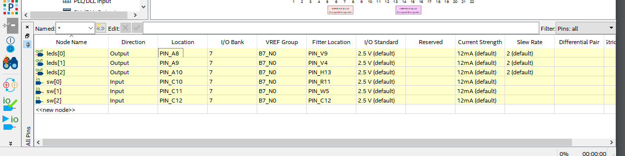
The assignment are saved automatically.
Compile again to make sure that you assigned the pins correctly.
Connecting Fpga and generate bit stream file
- In that section we will connect the fpga and created the configuration file called bit file of our design into the fpga.
- Please make sure that ypur fpga board is connected to your computer using the usb cable.
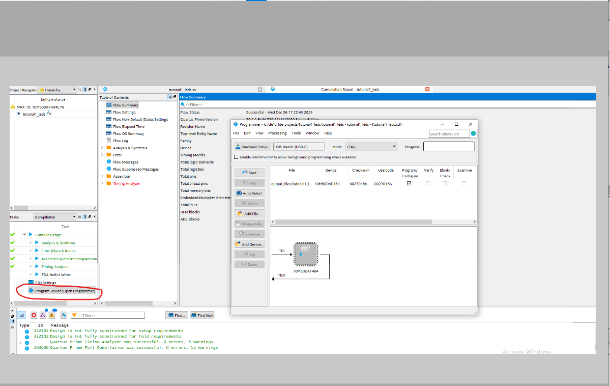
- At the compilation window double click on program device. and click start on the opened new window.
Trouble shooting
If its your first time you probably will have to install the drivers. For more details click here
After installing the driver, click Harward Setup and select USB-Blaster. Then click Close.
Now click Start again and wait until the process is finished. You will see a green check mark if the process is successful.
Play with the 3 right switches of the fpga and see that the leds are changing accordingly.